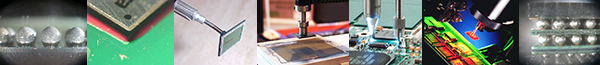
Solderability Benchmarking, Failures & Testing Methods
14th August
All our webinars are based on UK time you can check the time in your location Click Here
Benchmarking you PCB surface finish or the impact of baking boards or components can be simple in production and the laboratory. Long term solderability of component terminations and printed circuit boards is fundamental in modern assembly processes. This is all practical experience not just theory for the presenters countless studies in industry. Understanding how to conduct simple shop floor assessment of components or using laboratory test methods will be discussed along with artificially age coatings to simulate their useful life. Solderability can impact yield and reliability and making sure engineers understand the test methods onsite, or when subcontracting you’re testing to a laboratory, is key to ascertaining the correct root cause of your process problem.
The webinar will last approximately 60-90mins including a question and answer session for your process problems. If you have a specific process problems with reflow send it to Bob to include in the webinar
Topics covered:
Test specifications
Test methods
Selecting the best procedure
Ageing samples
Assessment of results
Solderability failures
The webinar material includes slides from the event, solderability testing wall charts and design files for solderability test board to use in your factory
PCB Outgassing and How to Test Bare or Assembled Boards
11th September
Printed circuit boards outgas during soldering causing solder voids, solder balls and other process problems. Outgassing can occur in wave, selective and reflow soldering and it’s important first to non-destructively test samples to find the root cause. It’s possible to test bare or assembled boards to examine the potential for failure and eliminate some of the popular misconception in industry. There some different methods which can easily be conducted in manufacture before proceeding to costly laboratory analysis and we show you how to do it and the typical results you can find!!
The webinar will last approximately 60-90mins including question and answer session
Topics covered:
Type of outgassing from vias, through holes and solder masks
How to Test samples in manufacture
Test method procedures
Type of defects and how they can appear with tin/lead and lead-free alloys
Void formation in wave selective and PIHR joints
Correct specification of your boards
A copy of the slides presented during the webinar are provided at the end of the event along with a written procedure for testing
Solder Shorts & How to Eliminate Them – In Selective & Wave Soldering
17th October
Solder short and unsoldered joints are fundamental defects in manufacture and can occur due to design, process change, change in materials or poor process set-up. Some fundamental choices in the methods of assembly and soldering process will increase solder shorts and this session will look at the causes and cures of the solder short
During the session, your presenter will show many causes of solder shorts forming and different solutions to the problem, both process and design tricks of the trade. Process tricks are particularly useful to the contract assembler finding it difficult to get design changes pasted customers. However, many changes in design are very simple, quick and will have no impact on function, reliability or product operation. Some suggestion allows for greater design density and reduce the possibility of product failure
Presented by Bob Willis who spent many years running the Electrovert Wave Soldering Master Class, both one and two-day theory and hands on training in Europe. Bob still runs his own courses on selective and wave soldering for customers worldwide
Each webinar last approximately 60-90 mins with the opportunity for questions on you process issues. Registered delegates on the webinar can send their own problem images for discussion during the webinar
Topics covered include:
Selective & wave soldering process
Flux activity & De-Activation
Solder drainage & cooling rates
Wetting speed
Design & layout
Solder shorts
Solder flags
Solder whisker
Impact of solder pallet design
Process optimisation
A copy of the slides presented during the webinar are provided at the end of the event
Ball Grid Array, Bottom Mounted Component Design, Assembly, Inspection & Defect Elimination
13th November
This webinar includes all BGA (Ball Grid Array), BMC (Bottom Mounted Components), PoP (Package On Package) component assembly and process setup with inspection methods and common failure detection and elimination. Bob produced the first training videos, interactive CDs on area array technology and the first book on PoP assembly and soldering
Bob’s session features many unique process video clips on testing and failures and make his sessions come alive providing a much better understanding of the root cause of failure and corrective action. A FREE copy of Bob’s Ebook on PoP is available to delegates and a copy of his area array posters is provided to each engineer attending this course
If you have a specific process problems with reflow send it to Bob to include in the webinar
Topics will include:
Package types
Design and PCB guide lines for parts
Assembly process options
Inspection standards
Common process and reliability failures
Defect Investigation techniques and corrective action
A copy of the slides presented during the webinar are provided at the end of the event plus a link to a text book on PoP assembly and inspection wall charts for QFN inspection