Having process problems, we solve process problems on a daily basis
So what are solder spots? They are often a problem in modern reflow assembly, in fact in any process that involves solder paste. The spots are visible on the surface of pads which have not been pasted prior to reflow. The spots are seen more commonly on copper, gold or any surface which is not fusible during reflow. The spots can be tin/lead or lead-free alloy which become visible due mainly to the different colour of the pad surface and the wetting action which takes place during reflow. If the spots were on a solder or silver surface there would not be much of a problem, out of sight out of mind. Some companies do apply rigid standards or apply the IPC guidelines very vigorously, failing the products at final test or during goods receipt if products are contracted out.
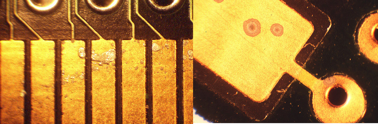
The images above are typical of solder spotting
Solder spots can be seen during a reflow simulation test using glass hour glasses placed over paste deposits on boards or test coupons then subjected to the reflow process. These samples allow any paste spitting to be visible after reflow on the surface of the glass. This test samples can also collect the volatile material from the surface of the board and paste deposit for analysis.
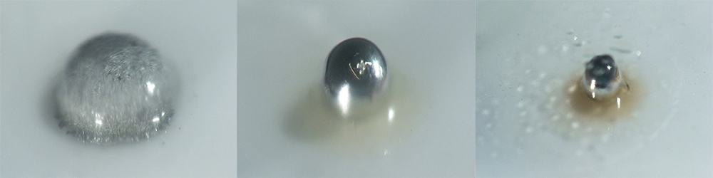
The three images above show the surface of the glass with the paste below in different stages of the reflow process. The final image shows the surface of the glass with the volatile material on the inside surface of the hour glass
If the surface of the pads is to be used for interconnection then any contamination may not be acceptable. Contact strips, LCD interconnection or key pads are examples where solder contamination of course, mechanical connection failure or intermittence. This would, have cause be related to the position and the size of the spots. It is, however much easier to just reject the products than make a judgment call but that is a costly option. Depending on the cost of the product, make repair viable the spots can be removed without any obvious signs.
If the spot is high off the surface of the pad concern may be shown on the effect on contact resistance on the switch pads. Any key contact or button contacting the surface may be lifted off the pad by the solder spot which will decrease the surface contact and increase the contact resistance. In most cases the contact resistance tolerance on such actions is wide and less likely to cause a problem. Surface analysis of the solder spots has confirmed that the spots are tin/lead and are most probably caused by solder paste particles. More detailed evaluation would be able to determine the alloy content and separate the hand cored wire, wave soldering alloy or even plating from component terminations. The particles present on the surface of the pads during reflow will wet the surface and it only takes the smallest of particles to have a visual impact on copper and gold features.
The surface spots can be seen as a random defect or consistently in the same position on the circuit pattern. They are very commonly seen at the edge of tacks and pads which is normally a fairly good indication of the root cause of the problem.
Elimination of the spot plague needs close consideration of each of the assembly stages in the modern factory. This is necessary as each could contribute to the problem of surface contaminates. So lets call in the spot inspector !
Screen Print
During solder paste printing thousands of small balls are printed on to the surface of the board in an attempt to produce consistent solder joints. During normal printing there are a number of things which make contact with the top and bottom surface of the board. The most obvious is the metal stencil which contacts the surface of the pads and depending on the pressure applied during printing, the surface of the board.
Solder paste will squeeze out between the stencil and the pad if a poor gasket is produced allowing paste to contaminate the base of the stencil. Recent video recordings produced by the author showing paste squeeze out due to uneven board surfaces show how much this can be a problem in manufacture. In this situation the paste particles on the base of the stencil can contaminate the adjacent areas of the next and future boards. When an under stencil wipe is used the particles can be spread around on the base of the stencil without being properly removed resulting in random spots after reflow. Care needs to be taken on the maintenance of the wiper cloth and the solvents used.
During printing supports are used to maintain the board flat and provide the ideal surface for printing. The board support may be a solid machined plate, groups of magnetic pins or specially moulded supports. In the case of the machined or moulded support or nests vacuum is normally used to help nest the board. Excessive suction has been shown to pull paste particles through the board to the base or along the surface of the board between the stencil. In each case this has resulted in surface contamination which can be random or in a line from a pasted pad feature to a via or hole where the vacuum pressure is seen. It is also most likely to be on the edge of pads.
There are very few examples of plating outgassing today but one example of a surface mount component I analyzed recently for a customer. The component terminations outgassed during soldering caused voids in the joints and local spots. This was originally blamed on the paste and reflow profile until the components were tested.
PCB Wash Off
One of the most common reasons for random defects is washed off boards. The board may look clean but a few solder balls is all it takes to cause solder spotting. If the board is poorly printed or there is down time on a production line boards may be washed off. When this is done paste particles can still be found in via holes, tooling holes and in resist apertures between the resist wall and the pad. This is why solder spotting is often seen at the very edge of the pads after reflow.
There have been many occasions where poor washing was the cause but every one said the boards had never been cleaned. “We never ever do that” said one contractor at an workshop only to be shown the particles in the solder resist undercut.
Placement
After components are placed into the surface of the paste the board should be reflowed and that is the operation complete. Misplaced components can be only just off the surface of the pad or completely misplaced. This can result in manual pick up of a part and repositioning it in its correct location. If the part has been in contact with the paste then the terminations will have paste on them. If the part was on another pad which is not pasted some paste will be left behind when the part is lifted. This would be totally random and very few companies have records of the occasional replacement exercise.
Printed Boards
There are times where the type of assembly or issues with the printed board can cause solder spotting during reflow. There are occasions when manufacturing engineers have printed solder paste into via holes to fill the via during reflow. This may have been done to provide a test pad, prevent vacuum loss during in circuit test or in an attempt to improve the reliability of the via. Paste printed into a via will reflow but what if the copper plating thickness is poorly controlled the via will gas causing the particles of paste to be displaced.
The same can be seen during pin in hole/intrusive reflow assembly. A large volume of paste in a confined space will prove difficult for the soak zone of a reflow process to allow the evaporation of the solvent. Again small particles can gas out causing random spotting.
Reflow
Some engineers have blamed the reflow oven for causing the paste to spit resulting in random spotting. Solder paste should not spit during reflow if the profile and the paste are compatible. To test your product simply take a hot plate and a pasted board and reflow the board on the plate matching the profile recommended by the solder paste supplier. This has been done in the past by placing shims between the board and the plate to adjust the ramp rate. The same test can be conducted in an oven during the normal reflow cycle but it does not provide the opportunity to record or observe the cycle, seeing is believing.
Take an hour glass plate normally used in a laboratory and place it over the board. The smaller the glass and the closer it is to the paste the better. This technique was originally used by the author to show when the different solvents in a paste evaporated during reflow. Normally condensation is seen on the surface of the glass. If any spitting were to occur with a paste this would be visible on the hour glass. An alternative is to use a white card when placed over a hot plate. The white paper or card trick is also used to assess some cored solder wires for spitting during hand soldering and is simple and cheap evaluation tool.
A number of engineers have considered the possibility of paste particles being circulated in the convection reflow oven, either due to high convection rates or re-circulating of gas at reflow or cooling phases. Poor maintenance of the equipment could, it has been suggested allow paste particles to fall onto the surface of passing boards prior to reflow. This is less likely due to the weight of the paste particles but can easily be determined. Production manager may not like it as throughput is king, but a problem needs to be sorted. Take a few sheets of thin copper laminate and, without any production running through the machine, pass the sheets repeatedly through the process. Inspect the panels after each pass for spotting.
There are still some companies who process double sided reflow products on mesh belts with the board in contact with the mesh during its second pass. A poorly maintained machine can easily have paste residues on the mesh which could contaminate the base of the board.
A final area to investigate are the entry and zone curtains on some ovens. The rubber curtains can, if incorrectly positioned or cut, will not only contaminate the board but displace components.
Finally don’t forget the wave soldering process if you find these defects at the end of the line. Its perfectly possible for solder to have reached the top side of the board. Caused by outgassing from the board, air knife pressure forcing solder out from tooling holes etc.
Rework
If solder paste is used during rework there is an opportunity for paste contamination. Normally paste used during rework is manually dispensed although some companies use mini stencils to apply the paste. This is a more obvious area for paste contamination and would normally be spotted quite quickly during investigation.
Finally just handling the boards in production should be avoided as any operator or technician knows paste gets everywhere. Generally when operators are using bare hands to handle boards they tend to be more careful with paste contamination. Some companies have the policy of wearing gloves which reduces the need for care as the paste will not go on your hands. Disposable gloves are used but they tend to cause sweating and not that well liked. The alternative reusable gloves tend to get dirty and again cause handling contamination.