National Physical Laboratory, NPL, has created an interactive assembly and soldering defect database, each month readers can add other defect solution to their own collection. Also available from the database is free access to over 100 process and reliability reports on soldering technology, Download Here
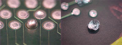
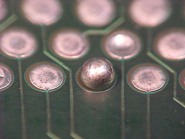
Solder balloons can be seen on the bottom of the board after wave or selective soldering and they can be attached to through or via holes as shown in the two examples. The solder balloons can be complete as in the first example or they have popped open. In x-ray you would see a complete ball but with a void inside the solder
Basically this process issue is caused by outgassing from the hole during soldering, gassing continues as the solder solidifies leaving a perfectly formed ball or popped balloon. It may be more likely to happen with a lead free solder that is not a true eutectic
Its fairly easy to test the board assembly or a bare board from the same batch with a high temperature oil to inspect for outgassing from the plating. Poor plating or thin copper plating of less than 25um can allow this process issue to continue
The main concern with this type of cosmetic defect is the high probability of the protruding solder ball catching on some surface during handling and the pad and track being lifted. Outgassing from PCBs is not uncommon but correctly specifying the board and having a copper plating thickness of 30um on through holes should avoid the issue. It is fair to say that as the via holes may have less copper plating in thicker boards we may still see balloons on our boards
To complement our “Defect of the Month” editorial Circuits Assembly now features “Defect Video of the Month” presented online by Bob Willis. This covers different failure modes with many video examples of defect occurring in real time and supported by IPC.
Martin Wickham is with the National Physical Laboratory Teddington, England defectsdatabase@npl.co.uk

