Supported by two of the industry’s leading magazines Circuits Assembly & Global SMT & Packaging magazine to help support engineers worldwide
Void Formation in Solder Joints – Causes & Cures – FREE Webinar
Wednesday 8th April 2.30pm UK Time
Book today
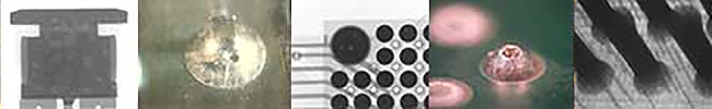
Voiding in solder joints is not new we have experienced cavities in solder joints during the introduction of through hole, surface mount and more recently area array technology. In many cases we never knew we have had voids till the introduction of x-ray inspection Voids can be created in solder joints; your speaker once had the job of creating voids to order in solder joint of a known size to aid inspection criteria. Voids can be seen in passive chip, J lead and gull wing and castellation terminations and we will show you how they form
Concerns were not really shown until area array technology started to increase in volume and with it the size of joints became smaller. Regardless of reliability voids or cavities on area array and large power devices will increase standoff, tilt devices and can mask other process issues This session will examine and demonstrate all of the common reasons why voids can form in solder joints. It will also highlight all of the inspection criteria in existing international standards. Plus we will shows void formation in underfill and adhesive joints
After the webinar there is a Q&A session which provides ample time for all delegate questions to be answered. However, if a delegate has a process example they would like covered in the webinar, it will need to be provided in advance of the session. The webinar will run for between 60-90min with question and answer session. The webinars are limited to 100 delegates/companies. A copy of each of the slides presented will be provided after the webinar