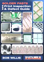
We are currently working on a new colour photo guide with “What’s New in Electronics” to illustrate solder paste printing defects often seen in surface mount manufacture. In addition the guide will cover most aspects of printing and inspection plus linked online video clips to better illustrate faults and how they occur during assembly. The guide will feature design mistakes which impact printing but then become more obvious when a product is reflowed
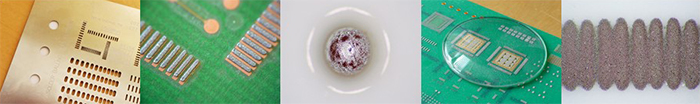
Example video above shows printing onto glass to show paste fill, stencil separation and final print deposit left left in the stencil, which is not desirable
If you would like to know more about the project and contribute please Contact Us Here
Topics Covered in the Guide and the online webinars – Book your place on the webinar
Solder paste storage and control
Printing solder paste
Stencils types, inspection & QC
First off print monitoring
Stencil cleaning, inspection & storage
Solder paste print inspection – manual
Paste printing defects
There are a couple of FREE online webinars to support the launch of the new guide where we may include a special discussion forum – Book your place on the webinar
 Bob has produced many illustrated defect guides over the years covering:
Lead-Free Assembly Defects
Conformal Coating Defects
PCB Surface Finish Defects
QFN & Area Array Defects
PCB Assembly Cleaning Defects
Low Temperature Soldering
Ball Grid Array Optical & X-ray inspection