The subject of outgassing, as it relates to printed circuit assemblies during the wave and selective soldering operation, has been an area of debate for many years. Until recently the soldering equipment often received the blame for pin holes and blow holes; the source of the problem was established many years ago. It is true to say that any soldering system would have to be operated well outside effective soldering limits with poor quality control for outgassing to occur
Outgassing can occur from solder mask, surface finishes and component lead plating but that is another article and can also be tested with other methods the author has used. We test boards and other material for customers as well as training staff to identify and undertake corrective action on materials and processes online or onsite
Over the years, a number of articles have been published which have put forward many suggestions as to the cause of the outgassing phenomenon. It was not until the involvement of the National Physical Laboratory (NPL), as part of the Soldering Science and Technology Club (SSTC), that any detailed scientific work could be co-ordinated at a national level. The club worked closely with major companies and with trade groups like the Joint Telecommunications and Components Working Group. The work of the joint activity highlighted the following points which have been shown to affect the degree of outgassing.
Blowholes and pin holes are caused by the escape of gas through the plated copper hole during the soldering operation. The gas is water vapour which is super heated during the soldering operation and escapes through the solder during its molten state. Voids are formed when the gas continues to escape during the solidification of the solder joint. On examination outgassing may result in pin holes, blowholes or sunken joints.
Outgassing can be eliminated if the copper plate is uniform in its thickness and is impervious to the gas escaping. This depends on many factors like the quality of drilling, the effective deposition of the electroless copper and the correct thickness of electroplated copper to resist the flow of escaping moisture.
The drilling may cause a problem due to the irregular surface that the copper will be required to cover and the need to bridge glass stands protruding into the through plating. This may provide voids which will allow continued gassing during the soldering operation.
Outgassing can be reduced during the soldering operation if the printed boards are baked prior to the soldering process. The baking operation must be conducted just prior to the assembly and soldering operation if it is to be effective in removing the moisture from the board. The boards must be baked at the correct temperature for the correct time duration to be effective. It should be noted that all glass epoxy is hydroscopic and will take on moisture during storage. This means that boards which have been baked need to be used if the baking operation is to be effective.
The incidence of outgassing can be eliminated by correct specification of the printed circuit board. Most national specifications quote a minimum thickness of copper plating in the through hole connection. The specification quotes a minimum of 20um but allows voids to also be present in the plating; this is, of course, a minimum standard which circuit companies in the main far exceed in terms of quality.
Many electronics companies can be accused of double standards. In the case of printed circuits they request boards to be manufactured to the national specification or, in some cases, have a company document which is slightly adapted from those specifications. In this situation they are implying that, in the worst case, they will accept boards which will outgass during soldering.
On the other hand the soldering standards operated in production, or imposed by a customer for second party manufacture, do not allow pin holes or voids so they are required to rework the solder joint to improve the cosmetic appearance. In no case has it been shown that touch up of solder joints improves the quality of the solder joint but in many cases the reverse has been shown; damage can be caused through repeated rework.
A simple non-destructive method of evaluating printed boards which may be conducted at goods receipt or during production is available on VHS video tape. Generally if outgassing is seen it will continue for a considerable time, in most cases until the heat source is removed; in cases during video filming the gassing has continued for over 1 min. The complete oil test and the results which may be obtained are shown on the video tape, the tape shows how the test is performed and the outgassing taking place. Where testing is conducted on a large sample size of boards a range of results will be seen. It is difficult in most cases to establish the size of the problem in the actual board but in situations where considerable gassing is seen it is easy to judge the effect it would have on manufacture. The method of test is very useful for demonstrating the phenomenon of water vapour escaping from both thin and voided copper plating. It can also demonstrate the likelihood of solder voids being seen in production. The test could be used as a criteria for the need for pre baking of the board prior to soldering but at best it can only be a guide.
The test has been successfully used in many companies to examine the effect of other manufacturing processes; its greatest benefit is its simplicity and its non destructive nature. Suggestions for its adoption as a standard test are unfortunately limited as who will specify the number of bubbles formed in a given time, the size of each bubble and the rate of escape?
NON DESTRUCTIVE EVALUATION OF PLATED THROUGH HOLES
The test is used to evaluate printed circuit boards with plated through holes for outgassing. It indicates the incidence of thin plating or voids present in through hole connections. It may be used at goods receipt, during production or on final assemblies to determine the cause of voids in solder fillets.
Provided that care is taken during testing the boards may be used in production after test without any detriment to the visual appearance or the reliability of the final product.
See examples of the outgassing test being conducted in our lab for customers plus many other Defect of the Month Videos
 https://www.youtube.com/user/MrBobwillis
TEST METHOD
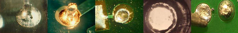
A sample board or part of a board is selected for examination. Each of the holes for examination are filled with oil; provided the oil is optically clear both visual inspection and photography may be undertaken. The best oil is available from any microscope supplier and referred to as optical oil used with an immersion lens. The oil is injected into each hole using a hypodermic syringe which makes it easy to perform and limits excess oil from being applied to the board. For effective examination it is necessary for the oil to form a concave meniscus on the surface of the hole to be examined. The concave form allows an optical view of the complete plated through hole. The easy method of forming a concave meniscus on the surface and removing excess oil is to use blotting paper.
In the case of any air trapment being present in the hole further oil is applied until a clear view of the complete internal surface is obtained. The sample board is mounted over a light source; this allows illumination of the plating through the hole. A simple light box or illuminated bottom stage on a microscope may provide suitable lighting.
A suitable optical viewing aid will be required to examine the hole during test. For general examination 5X magnification will allow viewing of bubble formation, for a more detailed examination of the through hole 25X magnification should be used.
The next stage of the test method is to reflow the solder in the plated through holes which also locally heats the surrounding board area. The easiest method is to apply a fine tipped soldering iron to the pad area on the board or to a track connecting to the pad area. The tip temperature can be varied but 500oF is normally satisfactory. The hole should be examined simultaneously during application of the soldering iron. Seconds after the complete reflow of the tin lead plating in the through hole bubbles will be seen emanating from any thin or porous area in the through plating. Outgassing is seen as a constant stream of bubbles which indicates pin holes, cracks, voids or thin plating.
Generally if outgassing is seen it will continue for a considerable time, in most cases it will continue until the heat source is removed. This may continue for 1-2 minutes; in these cases the heat may cause discoloration to the board material. Generally assessment can be made within 30 seconds of application of heat to the circuit.
After testing the board may be cleaned in a suitable solvent to remove the oil used during the test procedure. The test allows fast and effective examination of the surface of the copper or tin/lead plating. The test may be used on through holes with non tin/lead surfaces, in the cases of other organic coatings any bubbling due to the coatings will cease within a few seconds. The test also provides the opportunity to record the results both on video or film for future discussion.
TEST EQUIPMENT
- Sample Printed Circuit Boards For Evaluation
- Microscope with top and underside lighting. Alternatively a suitable magnification aid of between 5 to 25x magnification and a light box.
- Canada Bolson oil or suitable alternative which is optically clear for visual inspection and can be easily removed after test.
- Suitable hypodermic syringe for application of oil in each hole and blotting paper for removing excess oil.
- Soldering iron with suitable temperature control.