While the use of blind vias has become fairly common in electronics manufacturing today, inspection of via holes during fabrication is still problematic. We take a look at a simple and easy way of assessing blind vias that makes failure analysis easier to perform and produces less controversy. We have been using this technique with success to complement standard microsections, I think it’s easier to perform? There are of course more advanced methods to be used but at a price. Producing sections Focused Ion Beam using is an ideal tool to remove the possibility of damage, introduce other forms or contamination or feature damage. The methods are more analytical in their approach and out of the reach of many assemblers including PCB supplier. Normally these methods are only used when there is a disagreement between supplier and producer facing a court case
Watch one of our You Tube videos on Testing Via Holes
It has become common practice to use blind, filled and stacked vias in many portable electronics products. Experience has shown that this method of interconnection is reliable provided the fabrication process is well defined and controlled. Both through hole, blind and buried vias can stand-up to conventional and lead-free manufacture as the length of the barrel is short. It is, however, still difficult to inspect via locations during the fabrication process and there is often great debate on the cause of any failure or if a particular via is satisfactory of not. Much of this relates to the contact between capture and the plating, poor sectioning or etching methods can give different answers
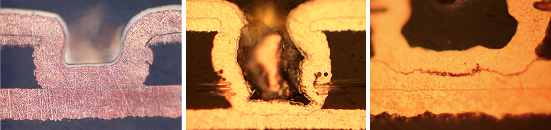
Images above show typical examples of via connections, not all are good
It was a little unfortunate that the IPC-A-600G did not address the issue of via assessment when it was last updated and released during 2004 but the recent revision 600H and J does include some guidelines. Blind and buried vias have been used in the industry for many years. Great experience exists, but very few standards or inspection guidelines exist for a company to reference. Very few users evaluate sample vias before and after thermal shock or focus on the quality control methods used in manufacture. Producing a microsection is still the most common method of via assessment. Engineers who have learned the procedures of microsectioning will state that it requires great level of skill and experience to correctly prepare and make assessment of a blind via. Often the assessment can be debated due to the methods of sectioning and the final etching process used on the copper layers. Engineers debate what may be an open or if it is simply a different copper interface. Electrical test before and after thermal shock or during thermal testing. This resistance was originally used to test changes in ductility on through hole multilayer test coupons in a fluidised sand bath to maintain consistent temperature on samples
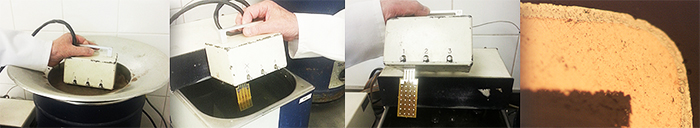
Images above show the use of sand bath testing of samples
Over the last year experience has been gained in using a different approach, or perhaps just coming at the problem from a different angle. Over many years engineers have produced traditional microsections looking at plated through holes along the length of the barrel. In the case of multilayer boards if any concerns are seen on barrel plating and inner foil separation, experienced engineers would turn the section around and examine the copper pad connection on half the remaining hole. Basically, we grind down vertically to obtain a different view
Examination of Blind Vias by Back Grinding
The following procedure may be used to examine blind and stacked via interconnections for routine testing or during failure analysis of a printed circuit board. The illustrations outline the typical procedure and the information that may be obtained from any via. A section of the board must be cut containing the via or group of via holes under examination. This can be conducted with a rotary diamond saw to minimise damage to the board or flexing thin substrates
Examination of the Gerber files can help to determine the points of interest provided the fault locations have been determined by electrical test or by using x-ray. The design files can also show other via positions in this layer. The board section must be cleaned in IPA to remove any surface contamination. This also ensures the mounting resin will adhere correctly during curing. Often if a no clean flux has been used or the joint areas have been reworked the amount of flux prevents resin bonding to the surface of the boards leaving voids in the section
The section of the board must be marked, or a reference diagram/photograph made so the correct via or vias are being examined always. The board section is then placed in a microsection mould. The position must be such that the back of the via or capture pad is facing down. The epoxy mix must be poured in slowly to cover and surround the section of the circuit board. The epoxy is simply being used to hold the board during the grinding operation. The section mould must be placed in an air circulated oven and the epoxy allowed to cure. When the epoxy is fully cured it is carefully removed from the mould and the exposed face of the board towards the back of the via hole capture pad must be ground. Grinding can be conducted initially using a 400 grit then reducing to a 600 grit paper to slow down the epoxy removal rate. Scratches are not really an issue in this procedure, but control of the depth is more important. When approaching the back side of the capture pad finer paper must be used to stop the copper trace and pad being mechanically removed ripped from the resin
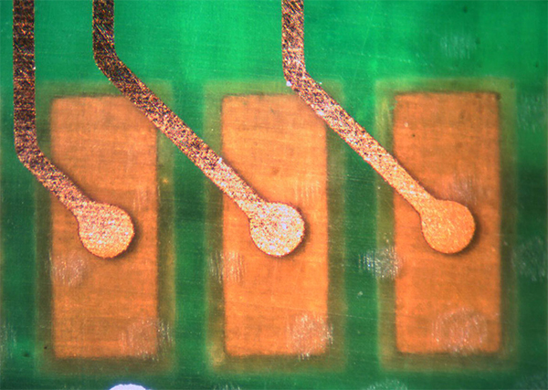
Examples of the via and track patterns visible through the PCB. The inter connected solder pads on the top of the board are also visible
The depth of grinding must be checked regularly with a microscope or 20x eye glass to determine when the pad surface is near. Ideally the objective is to reach the base copper foil surface or the epoxy layer just below the Copper track and pad. With care, and keeping the section flat, it should be possible to examine more than one via interconnection using this technique. If more than one via can be examined, then a better understanding of the quality of the interconnection and general fabrication process can be made. If this technique is only being used for failure analysis of a specific via other vias can be examined first without disturbing the via in question. They allow an engineer unfamiliar with the technique to practice on pad and via separation
When the section to the base of the copper foil has been ground, it must be placed under a microscope and the track end connected to the capture pad lightly probed. The track must then be peeled from the surface of the epoxy. If during grinding the copper surface is not reached, far more strain will be put on the track and copper pad during peeling. With experience an operator will be able to tell by the colour change when not covered in resin. Remember that the copper foil at this point may be just a few microns. When the copper track is peeled back, the capture pad will also be separated from the base of the plated via if there is intermittent bonding
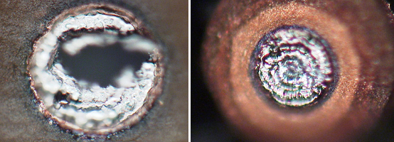
Images show one via separated in the copper barrel and the capture pad. The images above the capture pad with solder filling the via from the reflow process
The track and connected pad can now be placed in a sealed container for future examination; also the section can be placed in another sealed container. Correct storage of the samples prevents any debris falling on the two surfaces and possibly confusing any future analysis. Both of the mating surfaces of the blind via that have been separated can be carefully examined. First examination is conducted with a high magnification microscope to look at the previously mating surfaces. It should be possible to compare the surface of each and show how they have separated, if the copper plating to the pad was defective or not. The two surfaces should have features that match like two jigsaw pieces. Using an SEM, images can be taken of both mating surfaces. A mechanical break between two copper surfaces should provide a distinctive pattern allowing comparison on both surfaces. If the vias were correctly formed with a sound metallurgical bond but failed due to assembly or rework conditions, a hard brittle copper fracture would be noted. If the quality of the plating, hole and pad surface preparation was poor, then surface analysis on an SEM should be able to identify and characterise the surface. It could then compare with the surrounding materials
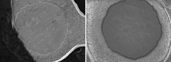
SEM images show the surface of the 0.020” 0.5mm capture pad (left) after separation from the bottom of the 0.010” 0.25mm blind via (right). There is no evidence of a fractured surface suggesting that a true bond could not have formed during the blind via plating process. Although no measurement of the force to remove the capture pad has been made, the bond was noticeably weaker than pads of the same size on known good vias
For help and assistance in your process problem Contact Us for a quick solution